mosfet band diagram
Band Diagram of Ideal MOS Structure at Equilibrium. 온라인 학위 학사 및 석사 학위 살펴보기.
Applied Sciences Free Full Text Atomic Layer Deposition Ald Of Metal Gates For Cmos Html
3-4 n-MOSFET Band Diagram.
. In general The body of the MOSFET is in connection with the source terminal thus forming a. Introduction to Semiconductor Devices 2. 332 MOSFET Flip-Flop Circuits131 333 Random Access Memory Devices.
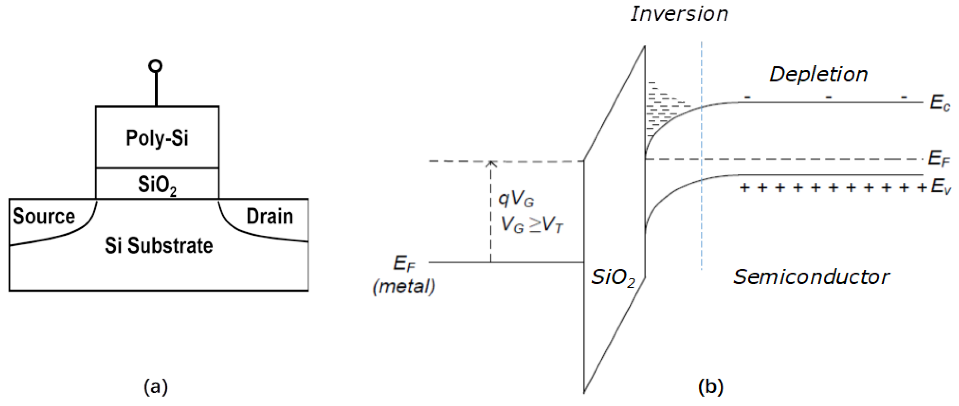
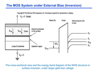
The energy band diagram of the p-type MOS device under inversion condition is shown in Fig. This clearly shows the existence of electric field. A MOSFET is a four-terminal device having source S gate G drain D and body B terminals.
3-2 MOSFET IV Equation Mobility Calculation ShortLong Channel MOSFET 1552. 3-4 n-MOSFET Band Diagram. Introduction to Semiconductor Devices 2.
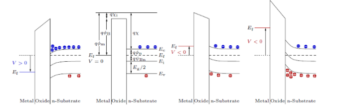
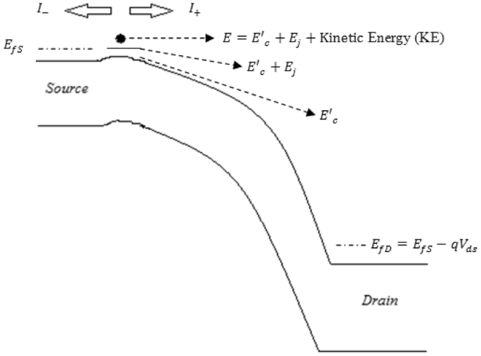
The energy band diagram for ideal MOS capacitor at thermal equilibrium with zero biased voltage condition is. 2 MOSFETs are barrier controlled devices the drain current is controlled by the height of an. ΦF VT Ln NA ni where VT KTq is thermal voltage.
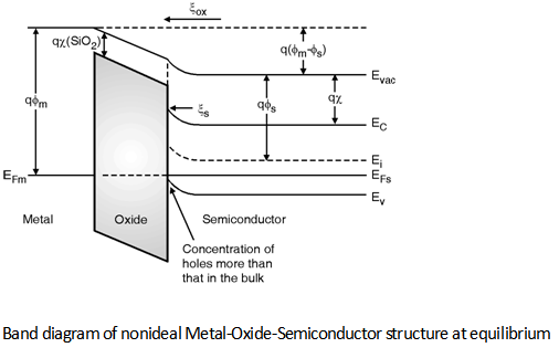
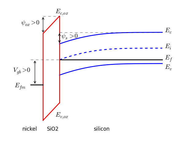
Hence the resulting electric field is. In the band diagram at semiconductor-oxide interface band bending occurs in the semiconductor side. MOS Capacitor band diagram question.
To understand the MOSFET we first have to analyze the MOS capacitor which consti-tutes the important gate-channel-substrate structure of the MOSFET. Once the location of Ei is known the conduction and valence bands can be. 1 Energy band diagrams provide a qualitative understanding of how MOSFETs operate.
The formation of this band diagram can conceptually think of the equilibrium metal-semiconductor. The MOS capacitor. Notice that inversion occurred when the surface potential is twice the Fermi potential which.
3-1 Metal-Oxide-Semiconductor Field Effect Transistors MOSFETs 2859. MasterTrack 修士号取得に向けて単位を取得 大学証明書 大学院レベルの学習でキャリアアップを目指す. Korea Advanced Institute of Science and TechnologyKAIST.
3-2 MOSFET IV Equation Mobility Calculation ShortLong Channel MOSFET 1552. The zero-bias band diagram in figure 2 a is called flat band diagram. MasterTrack 석사 학위를 따기 위한 학점 얻기 대학교 수료증 대학원 수준의 학습을 통해 경력을 쌓으세요.
3-1 Metal-Oxide-Semiconductor Field Effect Transistors MOSFETs 2859. In a MOS system is the energy offset between metaloxide or semiconductoroxide always the same regardless of the gate voltage.
Fermi Band Diagram In Mos Devices By Sukhanshu Dukare Medium
Band Diagram Of Nonideal Mos Digital Cmos Design Electronics Tutorial

Mosfet Wikipedia

Energy Band Diagram For The Three Possible Operation Regimes Of The Download High Resolution Scientific Diagram
Why Does Efm Shift In Mosfets Physics Forums
What Are The Energy Band Diagrams For An N Body Mos Capacitor In Accumulation Depletion Threshold And Inversion Regions Quora
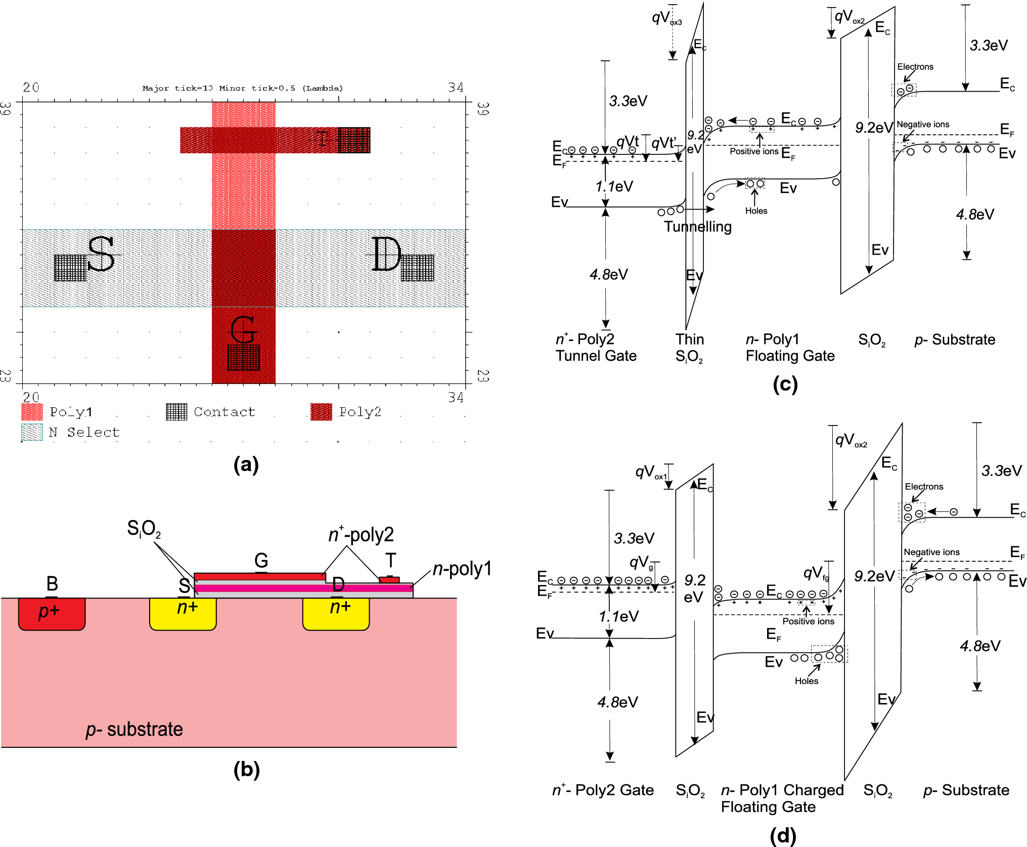
Figure 1 A New Floating Gate Mosfet Model For Analog Circuit Simulation And Design Springerlink
Automated Drawing Of The Mos Band Diagram
Monolithically Integrated Voltage Controlled Mosfet Led Device Based On A Gan On Silicon Led Epitaxial Wafer
Why Does Efm Shift In Mosfets Physics Forums

3 3 Mosfet Band Diagram Operation Mechanism Week 3 Coursera

Mosfet Band Diagram Explained Youtube
Solved Consider An Ideal Pchannel Mosfet A Sketch Energy Band Diagrams For The Mos Capacitor Under The 4 Distinct Biasing Conditions For Each Dia Course Hero
![]()
Band Diagram Tunnel Field Effect Transistor Mosfet Png Clipart Angle Area Band Diagram Diagram Electronic Band
![]()
6 Causes Of Mos Transistor Leakage Current Technical Articles

Band Diagram An Overview Sciencedirect Topics
A Quasi Ballistic Drain Current Charge And Capacitance Model With Positional Carrier Scattering Dependency Valid For Symmetric Dg Mosfets In Nanoscale Regime Nano Convergence Full Text